


If you didn’t guess it from the title, ISP is a way to serially program your microcontroller, while it resides in its place, in other words, without removing the chip from your board.
Whether you’re just starting in the ATMEL microcontrollers, or you’re familiar with it, ISP (In System Programming) will provide you a simple and affordable home made solution to program and debug your microcontroller based project.
Sometimes, ISP can become very useful, when adjusting some delays, frequencies or any other values that you would intend to find by trial and error.. a process that would otherwise take too much time.
How does ISP works?

Normally, the flash memory of an ATMEL microcontroller is programmed using a parallel interface, which consists of sending the data byte by byte (using eight independent lines for the data, and another bunch of lines for the address, the control word and clock input). On the other hand ISP is performed using only four lines, and literally, data is transferred through two lines only, as in a I2C interface, where data is shifted in bit by bit though.
MOSI (data input) line, with a clock cycle between each bit and the next (on the SCK (clock input) line). MISO (data output) line is used for reading and for code verification, it is only used to output the code from the FLASH memory of the microcontroller. The RST (used to activate the serial Programming) pin, which is normally used to reset the device, is also used to enable the three pins (MOSI, MISO and SCK) to be used for ISP simply by setting RST to HIGH (5V), otherwise if RST is low (0V), your program start running and those three pins, are used normally as P1.5, P1.6 and P1.7.
Here is ISP Programming sequence as described in ATMEL datasheets:
“The Code memory array can be programmed using the serial ISP interface while RST is pulled to VCC. The serial interface consists of pins SCK, MOSI (input) and MISO (output). After RST is set high, the Programming Enable instruction needs to be executed first before other operations can be executed. Before a reprogramming sequence can occur, a Chip Erase operation is required. The Chip Erase operation turns the content of every memory location in the Code array into FFH. Either an external system clock can be supplied at pin XTAL1 or a crystal needs to be connected across pins XTAL1 and XTAL2. The maximum serial clock (SCK) frequency should be less than 1/16 of the crystal frequency. With a 33 MHz oscillator clock, the maximum SCK frequency is 2 MHz.“
This is as deep as i got in the ISP process, as i am using a ready made software that will handle the transfer protocol. Some more detailed information about the ISP functioning can be found at www.8052.com and at But this is all you need to know to build and use this extra simple programming device. Now that you know some theory about the ISP, you should be ready to build the hardware interface. As you will soon discover, it maybe the simplest circuit that will find in this web site!
Circuit :

The circuit almost talks for itself, the only part that may need some explanation, is the four AND gates. Connecting both two inputs of the AND gates as shown makes it act like a buffer, to protect the parallel port (Shortly, a buffer is a device that will isolate two circuits).
Then, the pins P1,P2,P3,P4 have to be connected respectively to P1.5, P1.6, P1.7 and RST in the microcontroller.
Finally, J1 is the connection to the computer parallel port.
The PCB and the housing
I used an old parallel printer cable, and the whole circuit is mounted inside the the connector plastic box.
A glance at this pictures may be enough to understand how the PCB is mounted and welded to the parallel port connector. To achieve this, some precision have to be taken in account when producing the PCB.
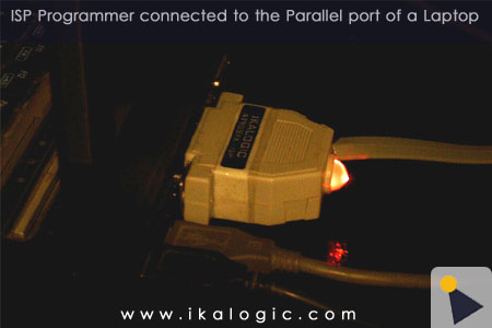
Here is a shot of the device in action. the picture may not be as clear as in reality, but i found the High Brightness LED to be cooler than what i’ve imagined..

Here is a shot of some other ISP programmers I made for some of my friends.


Connecting the programmer to the micro controller
Many visitors were confused on how to connect this programmer to the microcontroller. Well, in general, ISP is made to program the microcontroller while it resides in its place, so all the standard connection for the microcontroller to run properly are to be made.
As Mr Sarma – a regular visitor, reviewer and a friend – suggested, here are some examples showing how to connect the programmer to different types of microcontrollers:
- Connecting the programmer to an AT89S52

- Connecting the programmer to an ATMEGA16L
Note that with the ATMEGA AVR family, You don’t need to add a crystal resonator, as those chips contains an internal resonator, making it ready to use simply by connecting the 5V and GND supply rails.

The programmer software
 This is the piece of software that will take the HEX file generated by whatever compiler you are using, and send it – with respect to the very specific ISP transfer protocol – to the microcontroller.
The software I am proposing was designed to be compatible with a multitude of ISP programming cables. in most of cases, all the difference is the pins used on the parallel port to perform the data transfer. The only thing you need to do is to go through ‘Setup’, and chose the ‘AEC ISP’ cable pinout. once chosen, you will notice that it matches the circuit on this page.
If you have more than one parallel port (never seen this a lot..) chose the one to which the programmer is connected.


Tidak ada komentar:
Posting Komentar
Silahkan berkomentar !